How NASA's Quest for Smaller Space Cameras Created the Modern Smartphone Sensor
· GlobeWire Daily Editorial Desk · Source: www.techradar.com
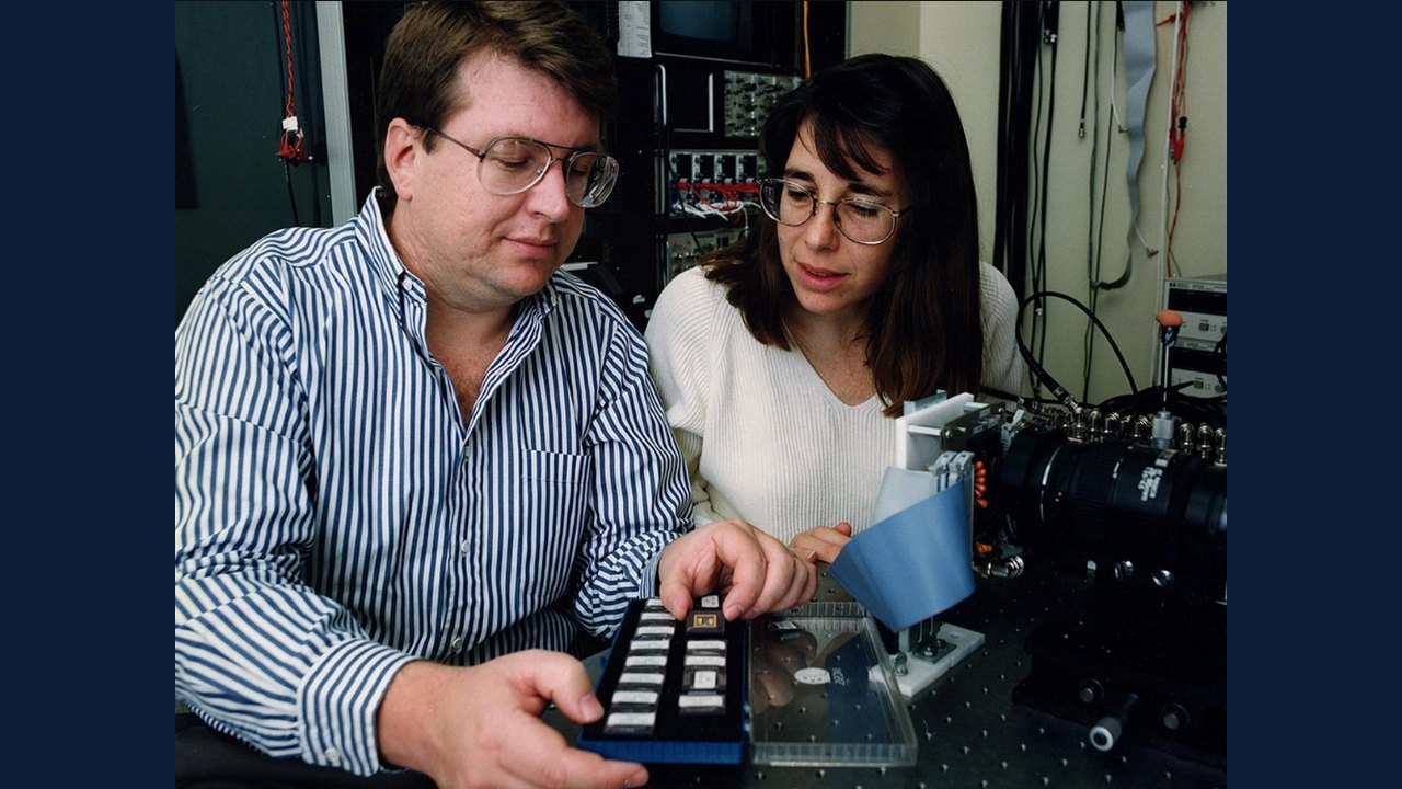
Image: TechRadar · Photo source · Resized and letterboxed to 16:9; no AI generation
Modern smartphone cameras trace their foundational technology directly back to space exploration initiatives from the early 1990s. According to historical accounts and engineering records, engineers at NASA's Jet Propulsion Laboratory (JPL) developed the CMOS active pixel sensor to significantly reduce the size and power consumption of cameras intended for spacecraft payloads.
The Origins of Space-Grade Imaging
In the early 1990s, then-NASA administrator Daniel Goldin advocated for a streamlined approach to space missions focused on making payloads faster, better, and cheaper. This directive placed heavy scrutiny on existing imaging hardware, specifically the dominant charge-coupled device (CCD) sensors of the era.
- The Problem with CCDs: CCD cameras relied on numerous separate components, consumed high levels of power, and integrated poorly with other electronics, making miniaturization extremely difficult.
- Historical Precedent: Earlier instruments, such as the vidicon cameras utilized on NASA's Voyager probes, weighed approximately 38.2 kilograms.
The Innovation of the CMOS Active Pixel Sensor
Led by engineer Eric Fossum, a JPL team developed the CMOS active pixel sensor by utilizing standard transistor technology common in computer chips. Previous attempts at CMOS imagers suffered from excessive image noise, but Fossum's team mitigated this issue using a technique known as intra-pixel charge transfer.
- Camera on a Chip: Because every individual pixel amplifies its own signal, supporting electronics can reside directly on the same piece of silicon.
- Power Efficiency: JPL documentation indicates that the new design required approximately one-hundredth of the power consumed by the legacy sensors it replaced.
Commercialization and Mobile Integration
Initial skepticism from industry peers and colleagues prompted Fossum and fellow JPL engineers to establish Photobit in 1995 to commercialize the technology. The company's chips eventually found applications in webcams and medical devices before being acquired by Micron Technology in 2001. Patent rights are currently managed by Caltech, with major manufacturers licensing the technology.
The commercial impact on mobile devices followed rapidly:
- First Integration: Sharp's J-SH04, released in Japan in November 2000, featured an integrated CMOS image sensor rated at 110,000 pixels.
- Market Growth: Industry estimates from Yole Group valued the CMOS image sensor market at $25.3 billion, with mobile devices accounting for approximately 63% of that revenue.
For further verification of historical accounts regarding NASA technologies, readers can consult official publications from NASA's Jet Propulsion Laboratory or review foundational engineering papers by Eric Fossum.
AI-assisted reporting; source claims are attributed and have not been independently verified.
More to read
 NASA Stennis Space Center Honors Employees at Annual Awards Ceremony
 NASA Outlines Coverage Plans for Upcoming Northrop Grumman CRS-25 Space Station Resupply Mission
 NASA Completes Construction of the Nancy Grace Roman Space Telescope Ahead of Planned Launch
 NASA Releases James Webb Space Telescope's First Full-Color Science Images